Developed by PCI-SIG®, PCI Express® (PCIe®) is a high-speed serial computer expansion bus standard that has been used in data-intensive applications such as data centers, AI/machine learning, HPC, automotives, IoT, and military/aerospace. Since the release of PCIe 5.0 and 6.0 in 2019 and 2022 respectively, PCIe has become even more common among modern motherboards and SSDs. However, not all PCIe designs are made equally — which is why we’ll be shedding light on key considerations and methodologies to help you optimize your design and test processes today.
A brief overview of PCIe standards
PCIe 1.0 was first introduced in 2003 at 2.5 GT/s. In contrast, PCIe 7.0 that is anticipated to be released in 2025 features an impressive speed of 128 GT/s, showing the remarkable progress that PCI-SIG has made in pushing the boundaries of data transfer rates. Innovations such as the transition from 8b/10b to 128/132 encoding between PCIe 2.0 and 3.0, as well as the adoption of PAM4 (Pulse Amplitude Modulation 4) in PCIe 6.0 have allowed PCI-SIG to double data rates with each generational release; spaced out over an average of three years each time.
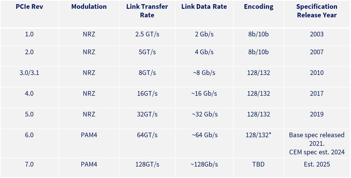
Figure 1: Evolution of PCIe technology
Last three iterations of PCIe (4.0, 5.0, and 6.0)
Comparing key differences across the last three PCIe iterations, we can see that the Nyquist frequency doubles between PCIe 4.0 and 5.0, while remaining unchanged in PCIe 6.0. However, the adoption of a different modulation scheme allowed PCIe 6.0 to feature a double data rate regardless. The insertion loss channel also increased between PCIe 4.0 to 5.0 while decreasing in PCIe 6.0, which was seen as a beneficial tradeoff for a doubled data rate.
The reference CTLE and DFE has also seen increase across all iterations to accommodate higher insertion loss or noise levels. Additionally, minimum scope bandwidth requirements have also increased. Calibrating receiver eye and testing in PCIe 4.0 only requires a minimum scope bandwidth of 25GHz. That threshold moves up to 33GHz for transmitter and receiver testing in PCIe 5.0, although receiver calibration and link EQ setup for the same standard requires 50GHz. For PCIe 6.0, 50GHz becomes mandatory for both calibration and testing.
Understanding the 3 different PCIe layers
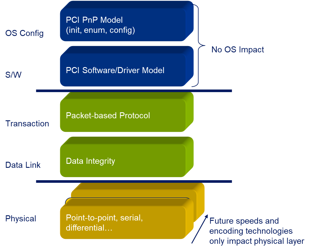
Figure 2: PCIe layers
First, lets understanding the roles of PCIe’s three core hardware layers:
- Transaction Layer (TL): Located at the top of the stack is TL which orchestrates data transmission and reception by implementing transaction flow control mechanisms and managing data packets’ transfer through the link.
- Data Link Layer (DLL): In the middle is DLL, which serves as an intermediary between the top TL and the bottom Physical Layer (PHY). DLL manages data framing, error detection, and flow control, while facilitating communication between endpoints.
- Physical Layer (PHY): This bottom layer consists of elements such as differential pairs and clock distribution mechanisms that facilitate data exchange. It governs electrical characteristics of the PCIe link, including signal transmission and reception.
Above the three core layers of TL, DLL, and PHY are software and operating system layers responsible for drivers and configuration tasks. While the software and operating system layers are also responsible for the overall functionality of PCIe devices, they are considered to be separate from PCIe hardware layers and are typically discussed within the context of software architecture and device management rather than the PCIe protocol itself.
PCIe Physical Layer
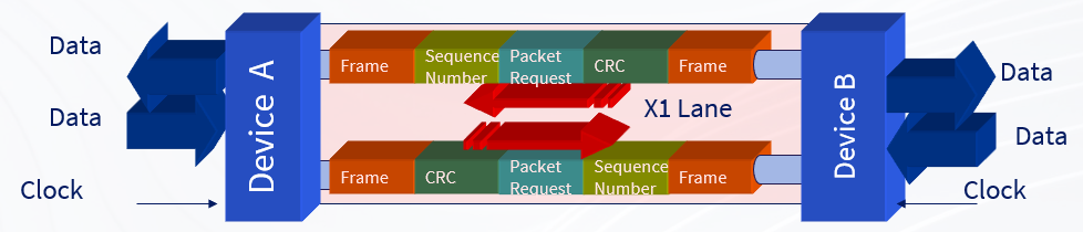
Figure 3: PCIe physical layer
In the PHY layer, a single PCIe link consists of two unique connection differential pairs between two point-to-point connections, supporting synchronization through embedded clocks. This architecture facilitates robust communication with support for SRIS and SRNS clocking schemes. Additionally, PCIe allows for various lane widths, including x1, x2, x4, x8, x12, x16, and x32, thus catering to different interconnection requirements.
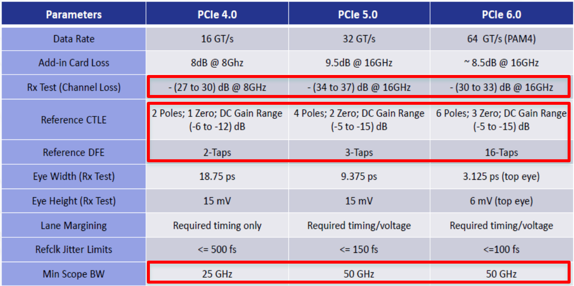
Figure 4: Parameters for PCIe 4.0, 5.0, 6.0
PCIe Base vs CEM specifications
The two key specifications in PCIe are Base and CEM. Both specifications differ significantly in test point definition, methodology, and degree of formality.
- Base specification: Defines electrical conformance at the chip level, containing technical details of the architecture, protocol, Link Layer, Physical Layer, and software interface. There are no official compliance programs or test fixtures.
- CEM (Card Electromechanical) specification: Defines mechanical requirements and electrical compliance for the completed product, i.e. Component (End Point, Bridge/Switch, Root Complex), Add-in Card or System (aka “Host”). Test fixtures and test tools are well-defined and supplied by PCI-SIG. Testing and compliance are governed by the Compliance Test Specification (CTS).
Whether you should follow the Base or CEM specification depends on your product's nature and customer base. Chip manufacturers primarily adhere to the Base specification, focusing on silicon-level testing and validation. End-product manufacturers follow the CEM specification, ensuring compliance with PCIe connector standards. There are also sub-specifications available for form factors beyond the Base and CEM specifications. which we will not cover in this article.
PCIe Compliance Program
The PCIe Compliance Program oversees the certification of PCIe products and ensures that the stringent PCI-SIG standards are met. Products must undergo testing either through PCI-SIG workshops or at authorized test labs to be certified and will be added to the PCI-SIG Integrators List upon successfully passing all Gold Suite tests and achieving an 80% passing rate for interoperability testing.
Currently, the Compliance Program extends only to PCIe 4.0 and 5.0 products, and only CEM form factors are supported for the official Integrators List certification testing. If you are looking to test other form factors, you will need to bring the right adapters to convert them to CEM during testing.
Test required for various product types include:
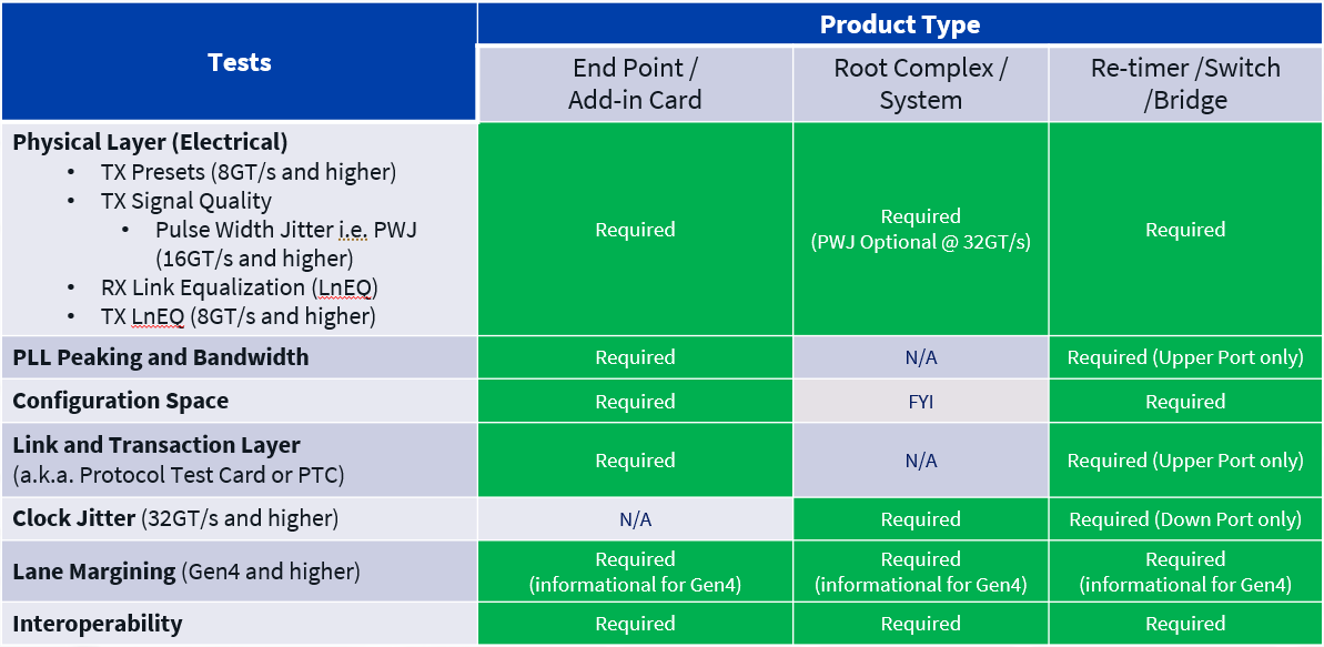
Figure 5: Tests required for different product types
Overview of transmitter testing for PCIe CEM specification
PCIe transmitter testing focuses on validating signal integrity and quality across various data rates.
The lanes to be tested depend on the configuration of the system. All transmitter presets for 8, 16, and 32 GT/s must be tested on lane 0 — the primary lane used for communication and configuration in a PCIe link. Signal quality and jitter tests are also conducted on lane 0, as well as on the adjacent lane (N-1) if present by using one qualifying preset. Configurations of greater than x4 will require lanes 0, N-1 and N/2-1 to be tested. The qualifying preset ensures that the transmitter is configured consistently for all lanes involved during testing, allowing for accurate comparison and evaluation of signal quality across lanes.
For example,
- For a x1 configuration, testing will be conducted on lane 0
- For a x2 configuration, testing will be conducted on lanes 0 and 1
- For a x4 configuration, testing will be conducted on lanes 0 and 3
- For a x16 configuration, testing will be conducted on lanes 0, 15, and 7
The RefCLK undergoes individual testing only for 32 GT/s systems. For all lower data rates, the RefCLK is indirectly tested while testing the transmitter signal quality. This is why for speeds of 16 GT/s or lower, a four-channel oscilloscope, also known as a two-volt test configuration, is necessary for comprehensive testing.
PLL peaking and bandwidth are tested on lane 0 only using Pulse Width Jitter (PWJ) and/or P7 compliance pattern.
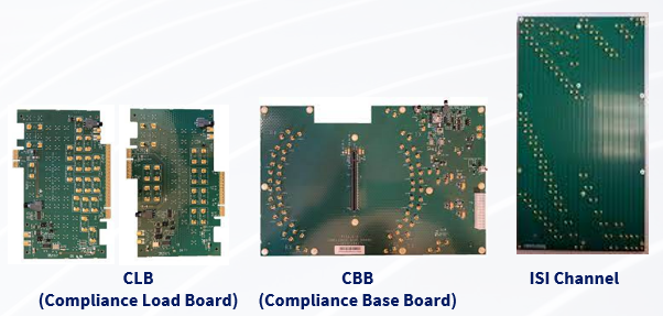
Figure 6: Official PCI-SIG test fixtures that are required for PCIe CEM transmitter tests
Overview of receiver link equalization testing for PCIe CEM specification
The objective of receiver link equalization (Link EQ) testing is to guarantee that the receiver under test can achieve a Bit Error Rate (BER) of 1E-12 with zero bit errors. The PCIe receiver Link EQ test procedure is as follows:
- Step 1: Calibration of the stress eye is performed for the required data rate (Figure 7)
- Channel Loss by VNA
- Eye Amplitude, Preset, SJ and RJ by BERT and RTO
- DM-I and Eye Height/Eye Width by BERT and RTO
- Step 2: Link Training
- Make DUT looped-back-mode by BERT through Recovery State
- Troubleshooting
- Step 3: Measurement of BER is done to achieve 95% confidence level
- Check BER <1E-12 with Stressed EYE (Mandatory)
- Jitter Tolerance Testing (Optional)
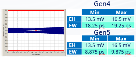
Figure 7: Minimum and maximum eye height and eye width requirements for PCIe 4.0 and PCIe 5.0 during calibration in PCIe receiver link equalization test
Watch the full webinar to see the test setup case studies in action
PCIe link and transaction layer tests
Beyond the physical layer, PCIe testing extends to the link and transaction layers, which address error handling and protocol compliance. The primary objective of link and transaction layer tests is to verify error handling at each layer, starting from the logical physical layer upwards. These tests aim to validate the implementation of capabilities and ensure their proper functioning.
Link and transaction layer tests include:
- Link layer tests
- Transaction layer tests
- Logical PHY layer tests (equalization protocol)
- Logical PHY layer tests (reserved bits in training sequence)
- Lane margining test - functional test
While the electrical PHY layer measures analog characteristics of the device to ensure proper signal transmission and reception, the logical PHY layer refers to the protocol used in the physical layer to adjust the electrical signals, which is actually a protocol mechanism. Hence, the logical PHY layer tests mentioned above are conducted with protocol test tools instead of electrical test tools.
PCIe link layer tests
Link layer tests in PCIe focus on evaluating various mechanisms to ensure proper data transmission and recovery across the PCIe link. These tests ensure that the link operates within specified parameters, including data rates, error detection, and error correction mechanisms.
Mechanisms that are generally tested in the link layer include:
- Replay timer / replay number / replay on NAK
- Bad data link layer packets (DLLP)
- Replay counter
- Bad Link Cyclic Redundancy Code (LCRC)
In the table below, you will find more examples of tests for the link layer. These tests are run with a Protocol Test Card (PTC) or an exerciser card.
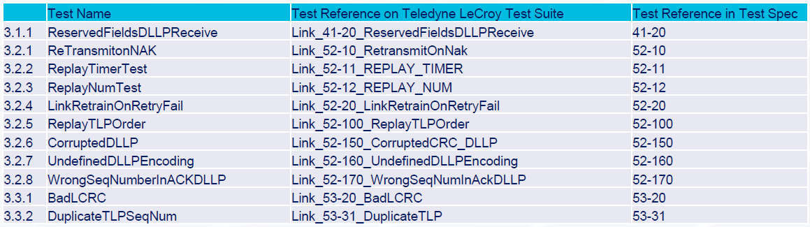
Figure 8: Examples of PCIe link layer tests
PCIe transaction layer tests
Transaction layer tests involve checking for errors in the transmission of the Transaction Layer Packets (TLPs). These tests cover scenarios like incorrect information within the TLP, ensuring request completion. Tests to detect poisoned TLP, wrong TLP sequence numbers, and nullified TLP are mandatory for PCIe compliance testing, while bad EndPoint Cyclic Redundancy Check (ECRC) detection is optional.
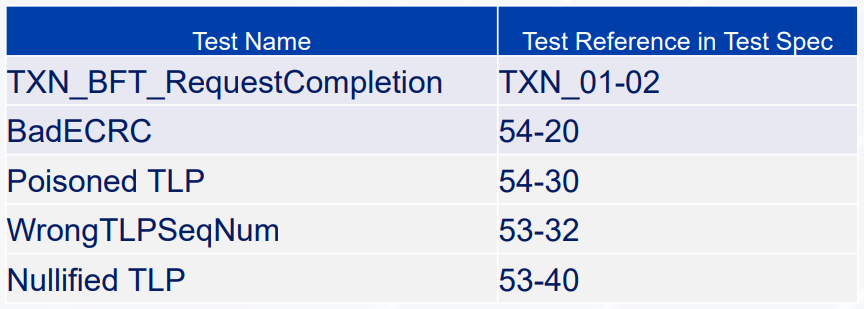
Figure 9: Examples of PCIe transaction layer tests
PCIe equalization tests (3.0 or higher)
When all connected devices in a PCIe link can support data rates of PCIe 3.0 or higher, link equalization will take place to optimize the connection and establish the most stable PCIe link at a higher data rate. As such, equalization tests must be conducted from PCIe 3.0 onward for all data speeds that the device supports.
- Adjust presets to ensure that response within training sequences are correct
- Run 55 different combinations of coefficients based on Full Swing (FS) and Low Frequency (LF) information of the device
The second step ensures that bad sets of coefficients are rejected and good sets of coefficients are reflected, and should be done for each data rate supported by the device.
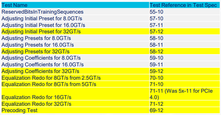
Figure 10: Examples of PCIe equalization tests
Watch the full webinar for more details on how PCIe 5.0 and 6.0 equalization tests differ
PCIe lane margining test (4.0 or higher)
Lane margining is a software mechanism that was introduced at PCIe 4.0 as an optional test that does not affect inclusion in the Integrators List. However, it has since become mandatory from PCIe 5.0 onwards.
Lane margining requires different steps to be conducted at different sampling points within the receiver to ensure proper implementation. When the host requests for margin information from the endpoint, verification is done by examining the numbers returned and how they relate to the margin.
While lane margining test is defined in the Electrical (PHY) Test Specification, it is run with the link and transaction tests for add-in cards in three different ways:
- Add-in card - no device driver required
- Add-in card - device driver required
- System lane margining testing
In system lane margining testing, electrical characteristics of the endpoint are changed and the resulting margins reported by the system will be measured. If a retimer or switch is present in the system, the test needs to measure the downstream facing retimer port connected to the slot or switch downstream port.
Test your PCIe designs at GRL
As the first PCIe Authorized Test Lab approved by PCI-SIG®, GRL will help you comply with PCIe specifications from 1.0 to 6.0. Speak with our experts to learn more. Still unsure about which test solutions you should use? Watch our full on-demand webinar to find out all you need to know about PCIe testing.