Simulation & Modeling
GRL offers the following Signal & Power Integrity modeling and simulation services:
- Channel Validation and Modeling
- System Level Simulation
- Equalizer Optimization
- IO model Validation
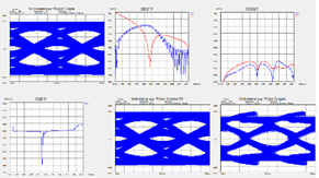
GRL offers Channel Simulation services to extract the model from your design layout.
GRL can also create/extract S-parameter models from physical passive channels: boards, connectors, and cables.
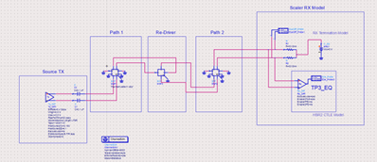
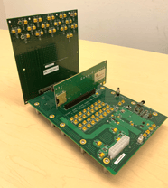
Channel topology gets complicated because multiple boards and connectors. GRL system level simulation services ensure that a healthy link between two devices is established through the channel.
GRL can help you successfully select implement re-drivers and repeaters into your design, including tuning and optimizing equalizer (EQ) settings to compensate for loss at every segment of the channel.
A long-time Keysight Solutions Partner, GRL leverages Keysight’s EDA tools suite including ADS, Momentum, and PLTS.
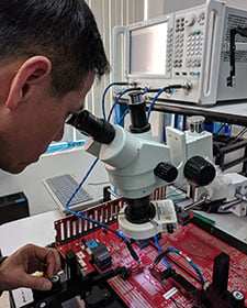
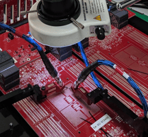
Lab Bench Measurement Services including Vector Network Analysis (VNA) & Time Domain Reflectometry (TDR) Analysis
- Board-level precision probing
- Cable & connector compliance and validation
- Fixture de-embedding / Custom de-embedding
De-Embedding Services
When you characterize a high speed signal you may need to use test fixtures or a dedicated test board with an embedded trace. These fixtures and traces have a non-negligible impact on GHz measurements. GRL can measure the “true” performance of your system using de-embedding techniques.
GRL’s comprehensive de-embedding services include:
- Consultation on how to de-embed components from the measurement
- De-Embedding Model Extraction
- De-Embedding Execution
Design Consulting and Custom Test Fixture Development Services
GRL offers comprehensive design consulting and troubleshooting support at the board, package, and system level.
GRL’s custom test fixture services include fixture architecture and turnkey design, manufacturing, and validation. GRL has helped many standards organizations and vendors with fixture design.
Contact GRL for a free consultation. Our experts will guide you through SI and PI design and validation from start to finish, covering via plating, layer stacking, and trace routing while keeping worst-case design and timing budgets into account to ensure optimal product performance.